ESP32 Mini kit pinout : is there a mapping table to Lolin ESP32 pinout?

Hi everyone,

I bought a couple of Wemos Mini D1 ESP-32S. It’s from the fabricant “MH-ET” and model MH-ET_LIVE_D1_mini_ESP32

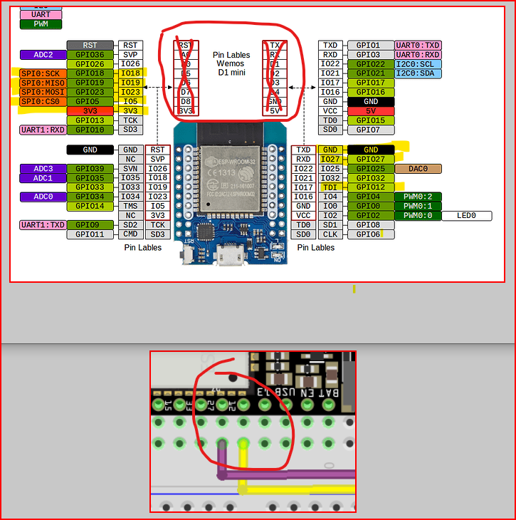
Apparently they have following pinouts

In the documentation, i.e.

I can read that I have to connect my CC1101 to following pinout’s: D27, D12, D18, 3V3, D23, D19, D5, GND, but … I don’t have this labeling on my ESP32…

Digging a bit further into the config files, I can see that i.e.

#  elif ESP32
#    define RF_EMITTER_GPIO 12 // D12 on DOIT ESP32

or

/*-------------------PIN DEFINITIONS----------------------*/
#ifndef RF_RECEIVER_GPIO
#  ifdef ESP8266
#    define RF_RECEIVER_GPIO 0 // D3 on nodemcu // put 4 with rf bridge direct mod
#  elif ESP32
#    define RF_RECEIVER_GPIO 27 // D27 on DOIT ESP32
#  elif __AVR_ATmega2560__
#    define RF_RECEIVER_GPIO 1 //1 = D3 on mega
#  else
#    define RF_RECEIVER_GPIO 1 //1 = D3 on arduino
#  endif
#endif

So my conclusion is that I need some mapping between D27, D12, D3 and the GPIO’s on the ESP32.
(I already noticed that I can NOT use GPIO27 as RF-receiver on my MH-ET_LIVE_D1_mini_ESP32, I had to use another GPIO. I don’t know why, but this is off-topic here).

Now I want to use my CC1101 on my ESP32 (MH-ET_LIVE_D1_mini_ESP32), but -apart from 3V3 and GND- I have no idea how I have to connect both devices.

Can somebody point me in the good direction?

How can I deduce which pins of my CC1101 should be connected to the GPIO’s of my ESP32?

Or how can I map the documented D27, D12, D18, 3V3*, D23, D19, D5, GND to the GPIO’s of my MH-ET_LIVE_D1_mini_ESP32. Is there such a mapping table for my MH-ET_LIVE_D1_mini_ESP32

thanx in advance!

Bart Plessers

The wiring of a CC1101 is documented here - RF gateway (433mhz/315mhz) | OpenMQTTGateway v1.4.0

I know, but that’s my whole point: in the documentation they mention D1, D3, etc
But my ESP32 has only GPIO1, GPIO2 etc…labeling.
So what’s the correlation between Dx and GPIOy?
In the picture above, they give a mapping for D0, D1, D2, D3, … D8. But not for higher Dx connectors

Hi @BartPlessers,

Just out of curiosity - have you tried hooking it up with the wiring description of the ESP8266 (very similar to the D1 mini ESP8266 wiring from LSatan, save for D2/RX) and defining them appropriately in your custom environment?

@BartPlessers With an ESP32 it is a direct mapping between GPIO number and D numbers, no funky translation needed. GPIO1 = D1 etc

Really???
The information from their website suggests following :

So
D0 - GPIO26
D5 - GPIO18
etc…

Sorry I’m not directly familiar with the board you are using, but for OMG we using this pinout

GDO2 - GPIO27
GDO0 - GPIO12
SCK - GPIO18
VCC - 3V3
MOSI - GPIO23
MISO - GPIO19
CSN - GPIO5
GND - GND

2 Likes

ah, super!
That is what I was looking for.

I’ll give it a try and let you know if this works on my device

grtz
B

@BartPlessers do you mind sharing your final pin out that worked for you?

I know that this is an older thread but this was never really answered and there may be others finding this and having the same question.

On a Wemos D1 MINI (esp8266), you’ll see pins 5V, GND, 4 & D3 (and four more.) The D4 and D3 are GPIO2 and GPIO0, respectively. But on a Wemos 32 D1 mini, you see the innermost pins on the right that have white around them (on the board itself) are 5V GND, D4 & D3 but they are also labeled as VCC, GND, IO16 & IO17. So the pins in white are the same layout (5V, GND, four general IO, RXD and TXD) on both boards so they can use the same hats. But because the actual GPIO numbers are not the same, you need the code adjusted for the pins/CPU. So if the code has “#define CLK 2” (GPIO2 or D4) for the esp8266, it’d need to be “#define CLK 15” for the corresponding pin on the esp32, etc if you want a 1-to-1 mapping of the physical locations on the Wemos esp8266 D1 and the white pins on the Wemos esp32 D1.

But when you’re seeing code for an esp32, D4 is never mapped to GPIO2 like it is on the esp8266. D4=GPIO4, D6 is GPPIO6, D1 is GPIO1, etc.

So ignore the two groups of pins outlined in red in the pinout diagram directly above the board as far as GPIO numbers go and directly convert “D27, D12, D18, 3V3, D23, D19, D5, GND” to “GPIO27, GPIO12, GPIO18, 3V3, GPIO23, GPIO19, DPIO5, GRD” (D5 being the one oddball because it’s the one showing as “SPI0:CS0 GPIO5 IO5” on the inner-left and corresponds to the ignored D8 on a esp8266 D1.) So the pins you’d need are highlighted in yellow in the upper part of the image.

You can confirm this in the documentation you links to (and shown in the second part of the image here) where they show a different esp32 board and using (GPIO) 27 and 12.